

MEMS, Microscopy and Microanalysis
From lab optics to industrial speed.
MEMS innovation – delivered with EQ Photonics.
When precision actuation and beam control must outperform conventional solutions:
- Access to a curated portfolio of high-performance MEMS components for advanced microscopy
- Expert support grounded in proven MEMS-based system development
- Feasibility testing included – tailored to your beam steering or scanning application

Maximilian Abeln – Sales & Business Development Manager MEMS Solutions
Successful projects – customers who trust EQ

Typical challenges when selecting industrial MEMS solutions
Standard solutions do not fit your unique application needs
High integration effort with existing lab system setups
Ensuring hermetic sealing, chemical compatibility, and stable behavior across environmental cycles.
Vendors offer generic parts instead of trailored solutions
Slow feedback loops delay prototyping and testing cycles
Difficulties with contactless quality control or position determination
Technology-agnostic MEMS consulting for microscopy and advanced applications
EQ Photonics supports you in selecting and integrating the right MEMS solution — from in-situ electron microscopy to custom sensor platforms. With vendor-neutral consulting, one of the widest technology networks in the market, and a deep understanding of real-world constraints, we help you turn complex requirements into successful outcomes.
Advanced Microscopy Solutions for Research and Industry
From high-resolution optical modules to integrated imaging platforms – EQ delivers tailored microscopy systems to meet the most demanding applications in life sciences, materials analysis, and industrial inspection.
Reliable Development through Individual Feasibility Testing
Before launching your project, we help validate technical feasibility through precision test procedures, ensuring compatibility with MEMS structures and advanced optical setups.
Rapid Prototyping and Flexible Support for MEMS-Based Projects
With deep expertise in MEMS integration, fast turnaround times, and transparent processes, EQ supports your custom device development from concept to prototype – with responsive service every step of the way.
Our products for microscopy and diagnosis at a glance
In-Situ
Heating Chips
Electrochemistry
Chips
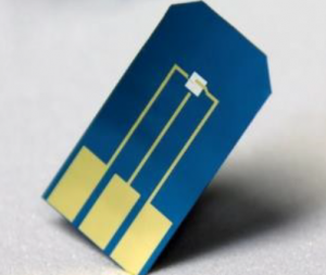
E-Biasing
Chips
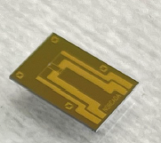
Heating Holders
Transmission Windows
Biasing Holders

What customers have achieved with our MEMS: Examples from the field
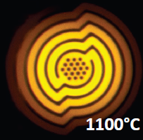
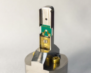
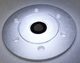
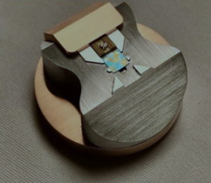
Precise Microscopy Inspection Using Sample Holders
3D visualization and analysis under extreme conditions
Use case: Investigation of nanostructured materials under high vacuum and low/high-temperature conditions
Key result: Reliable measurement in microscopy setups using sample holders for maximum stability and thermal control
Our service: Consulting service for selecting suitable chips, integration into existing systems, and optimization for maximum image quality
A leading research institute in materials science uses our solution to study 2D materials such as graphene and MoS₂. With Norcada’s microscopy chips featuring integrated heating and cooling technology, it is possible to precisely analyze samples at temperatures from -190 °C to +400 °C. The chips offer exceptional planarity and mechanical stability, enabling high-resolution TEM and SEM imaging without drift or thermal expansion. The result is significantly improved reproducibility and image quality in demanding analytical procedures.
.
SEM Analysis of Biological Samples Using Conductive Norcada Chips
Surface characterization at low electron energies
Use case: SEM of sensitive biological materials without damaging the sample
Key result: Stable sample preparation using conductive chips to avoid charging effects
Our service: Provision of customized conductive membrane carriers for sensitive organic or biological samples including full application support
A biotech company studied cellular structures using low-energy SEM (1–5 keV), which imposed strict requirements on sample stability and charge dissipation. Our solution involved specially coated Norcada membrane carriers with a thin gold or ITO conductive layer. This allowed the samples to be analyzed directly without additional sputter coating. The membrane carriers significantly reduced sample charging and delivered sharp SEM images with high contrast depth. The customer solution not only enabled a faster workflow but also allowed the analysis of living cells in dehydrated environments – a breakthrough in biological sample structure characterization.
High-Resolution X-Ray Characterization Using Membranes
Precise material analysis with X-ray microscopy under minimal background scattering
Use case: X-ray analysis of ultrathin materials and nanostructures with minimal substrate background
Key result: High-contrast and low-noise X-ray data using ultrathin Si₃N₄ membranes (<50 nm)
Our service: Selection and supply of application-specific membrane carriers including vacuum compatibility and radiation shielding consultation
A research center in the field of quantum-based materials development uses our membrane carriers for synchrotron-based X-ray absorption spectroscopy (XAS) on 2D materials. Crucial to the success was the extremely low background scattering achieved by the ultrathin 30 nm Si₃N₄ membrane, which offers high transparency to soft X-rays. The special geometry of the Norcada frame also allowed for seamless integration into existing sample holder systems. The resulting X-ray data showed a significantly improved signal-to-noise ratio and enabled quantitative conclusions on oxidation states and bond lengths.
This is what you can expect from us and our MEMS solutions:
High-performance microscopy
EQ Photonics, together with Norcada, enables advanced microscopy solutions through precision MEMS devices and optical components. These technologies open new possibilities in life sciences, material research, and nanotechnology by providing reliable, high-resolution imaging platforms.
Flexibility through modular and open platforms
Our microscopy solutions are built on open and modular designs, allowing seamless integration of MEMS chips, custom optics, and detection systems. This flexibility makes them ideal for research institutes and industrial labs that require scalable and adaptable setups.
Sustainable investment for cutting-edge research
With Norcada’s MEMS expertise and EQ Photonics’ optical know-how, customers gain long-term value through highly reliable components, upgradeable systems, and scalable designs. This ensures future-proof research capabilities in areas like single-cell analysis, spectroscopy, and quantum technology.
Who we are: EQ Photonics is your technology partner for MEMS solutions
EQ Photonics is your trusted partner for advanced photonics and MEMS-based solutions, offering manufacturer-independent consulting and deep technical expertise.
We bring together scientific know-how and market insight to make complex photonic applications—such as spectroscopy, quantum sensing, and X-ray analysis—accessible and scalable. Our portfolio extends far beyond imaging: EQ Photonics supports customers with modular component selection, system integration, and personalized project guidance that prioritizes your specific requirements—not off-the-shelf solutions.
| Manufacturer | Online-Shops | EQ Photonics | Consultant | |||
| Expert advice on customized solutions | ✓ | – | ✓ | ✓ | ||
| Integrated solutions from a single source | – | – | ✓ | – | ||
| Single point of contact for all matters | – | ✓ | ✓ | – | ||
| Access to research and development, product management and production | ✓ | – | ✓ | – | ||
| On-site training and support | ✓ | – | ✓ | ✓ | ||
| Delivery of small batches | – | ✓ | ✓ | – | ||
How to start your MEMS project with EQ Photonics
1. 30-minute initial consultation
2. Requirements analysis and application-specific advice
3. Joint feasibility test
4. Proposal phase and project start
5. Delivery, integration and support
Why does EQ Photonics rely on Norcada?
EQ Photonics has been working with Norcada for over a decade since 2015:
Norcada products impress with their technological precision, customizable design options, and strong performance in advanced photonic and MEMS applications.
Long-term availability of high-precision components for reliable integration
Broad selection of MEMS and photonic devices for diverse applications
Excellent performance-to-price ratio for research and OEM use
Flexible design options enable seamless system integration
Scalable solutions from prototyping to series production
Frequently asked questions about EQ Photonics MEMS products
Every application is different—whether you’re operating in high-vacuum, integrating into a quantum sensor, or conducting spectroscopy. Our team will evaluate your specific needs and guide you to the optimal Norcada component, including options for coatings, frame materials, and custom geometries.
Norcada offers a wide range of customization options including membrane thickness, window size, chip shape, material type (e.g. SiN, SiC), and coating choices. This flexibility allows us to tailor each component to your application’s exact requirements.
The price depends on the scope of the project, accuracy requirements and system complexity. In general, you will receive an indicative price range from us before the feasibility test.
Absolutely—EQ Photonics collaborates closely with customers during feasibility phases by supplying Norcada samples, offering technical consulting, and helping interpret results. Norcada products are widely cited in peer-reviewed scientific publications, confirming their proven performance in demanding applications.
We do not rely on standardized sales processes, but on individual support and technical expertise at eye level. We offer you technology-agnostic advice, a more diverse portfolio and significantly more in-depth solutions – from the initial consultation to the final solution.